My Research and Inventions

click here to see all content

 
Surface Plasmons

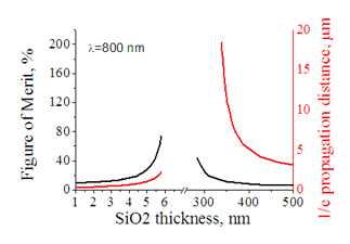
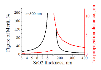
Plasmonic waveguides on GaAs substrate (wavelength: 800 nm)

Numerical examples. Enhancement of MO effect in the case of double-dielectric single-surface slab plasmonic waveguide.

Goal: To study and understand the features and properties of surface plasmons near cutoff condition.

Reason: The cutoff conditions in a double-dielectric plasmonic waveguide have never been studied before.

Note: The properties of plasmons near cutoff in the case of thinner oxide thickness (5nm -12 nm) and in the case of thicker oxide thickness (200 nm -900 nm) are significantly different.

need to know: To understand cutoff condition in dielectric waveguide click here


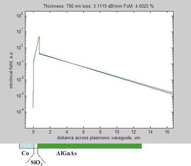
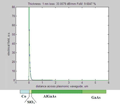
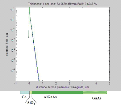
MO enhancement in the case plasmons (general fact are here)
Experimental confirmation of low optical loss in Fe:SiO2:AlGaAs waveguide is here
Below the data are calculated for a slab single-surface double-dielectric plasmonic waveguide.
Metal should be thicker than 3 skin depths (~ 100 nm)


GaAs substrate (lambda=800 nm)

Below it is the case when AlGaAs layer is sufficiently thick that there is no influence of GaAs substrate
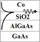
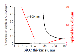
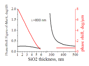
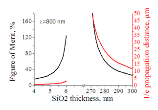
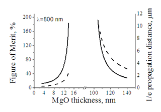
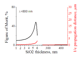


Optical confinement near cutoff

example: Co:SiO2:AlGaAs (lambda=800 nm)

In double-dielectric plasmonic case (In studied case it is semiconductor-oxide-metal plasmonic waveguide. See the numerical examples above) there always there is two cutoff thicknesses of the oxides. The surface plasmons can propagate only in the case when the oxide thickness is thinner than the thinner cutoff thickness(~ 5-12 nm) or thicker than the thicker cutoff thickness.

  thinner cutoff thickness thicker cutoff thickness
plasmon's effective refractive index ~ refractive index of semiconductors (~3.1) ~ refractive index of oxide (~1.7)
1/e penetration depth into dielectric medium (~ 2 um) very deep (~ 20um)
optical field near metal medium high
MO FoM high (~100 %) high (~100 %)
optical loss low( less than 1 dB/um) - average low( less than 1 dB/um) (experiment: 0.38 dB/um)
required precision for oxide thickness high (~0.2-0.4 nm) medium (~10 nm-15 nm)
non-reciprocal phase shift medium (0.5-8 deg/um) medium (0.7 deg/um)
FoM for non-reciprocal phase shift low (0.2 deg/dB) medium (2 deg/dB)
1/e penetration depth into metal (skin depth) 22.6 nm 25.5 nm

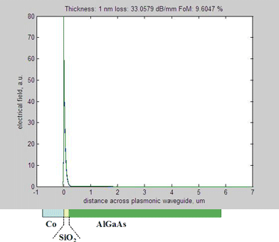
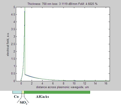
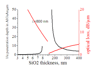
Examples below is for Co:SiO2:AlGaAs (lambda=800 nm) plasmonic waveguide.


cutoff: thinner SiO2

Optical field across plasmonic waveguide (normal scale)
Optical field across plasmonic waveguide (logarithmic scale)

cutoff: thicker SiO2

Optical field across plasmonic waveguide (normal scale)
Optical field across plasmonic waveguide (logarithmic scale)
Fig.1 Animated figure. Field distribution along thickness of plasmonic waveguide. Both linear and logarithmic y-axis scale are used. Animation parameter is thickness of SiO2 layer. The distance=0 corresponds to a metal-SiO2 interface. The blue and green lines correspond to opposite magnetization of Co.

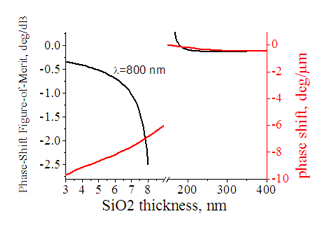
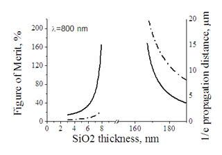
The important difference between distributions of optical field of plasmons near two cutoff thicknesses is that in the case of thick SiO2 a significant amount of optical field is confined inside this layer. It is reason of lower optical loss in this case. The more optical field is inside dielectric and the less optical field is inside metal, the smaller optical loss of plasmons will be.


Fig.3 1/e penetration depth of optical field into dielectric and optical loss in Co:SiO2:Si plasmonic waveguide

Fig.4 Non-reciprocal phase shift and Phase-Shift FoM (ratio of the phase shift to optical loss) for Co:SiO2:Si plasmonic waveguide Fig.5 MO Figure-of-Merit (Ratio of non-reciprocal optical loss to average optical loss) and 1/e plasmon propagation distance for Co:SiO2:Si plasmonic waveguide


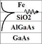
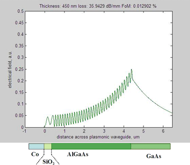
example: Fe:SiO2:AlGaAs (lambda=800 nm)

Fig.3a 1/e penetration depth of optical field into dielectric and optical loss in Fe:SiO2:AlGaAs plasmonic waveguide

Fig.4a Non-reciprocal phase shift and Phase-Shift FoM (ratio of the phase shift to optical loss) for Fe:SiO2:AlGaAs plasmonic waveguide Fig.5a MO Figure-of-Merit (Ratio of non-reciprocal optical loss to average optical loss) and 1/e plasmon propagation distance for Fe:SiO2:AlGaAs plasmonic waveguide


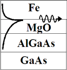
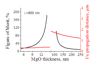
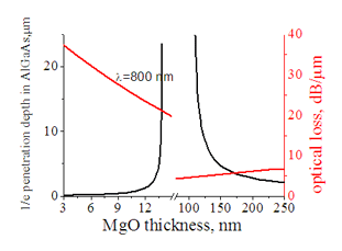
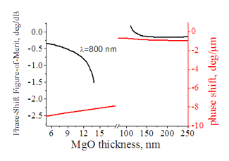
skin depth: 31.9 nm / 35.9 nm


example: Fe:MgO:AlGaAs (lambda=800 nm)

Fig.3b 1/e penetration depth of optical field into dielectric and optical loss in Fe:MgO:AlGaAs plasmonic waveguide.

Fig.4b Non-reciprocal phase shift and Phase-Shift FoM (ratio of the phase shift to optical loss) for Fe:MgO:AlGaAs plasmonic waveguide Fig.5b MO Figure-of-Merit (Ratio of non-reciprocal optical loss to average optical loss) and 1/e plasmon propagation distance for Fe:MgO:AlGaAs plasmonic waveguide


skin depth: 32 nm/ 35.5 nm

Finite thickness of AlGaAs

example: Fe:MgO:AlGaAs(4 um):GaAs (lambda=800 nm)

In this case optical field interacts with GaAs, which is an absorber at this wavelength and it modifies cutoff conditions.

Optical field across plasmonic waveguide (normal scale)
Optical field across plasmonic waveguide (logarithmic scale)

Fig.6 Animated figure. Field distribution along thickness of Co:SiO2:AlGaAs(4 um):GaAs plasmonic waveguide. Animation parameter is thickness of SiO2 layer. The distance=0 corresponds to a metal-SiO2 interface. The blue and green lines correspond to opposite magnetization of Co.

Fig.7 Animated figure. The same as Fig.7, but the y-axis is logarithmic Fig 8 MO Figure-of-Merit and 1/e plasmon propagation distance for Co:SiO2:AlGaAs(4 um) GaAs plasmonic waveguide. There is MO enhancement near thickness of SiO2 of 5.7 nm


The finite thickness of AlGaAs makes plasmons to interact with GaAs substrate. It has a negative effect on MO properties of the plasmons. As was shown above, the 1/e penetration distance of plasmon optical field into dielectric is about 1-3 um for thinner thickness of dielectric and 10-30 um for thicker dielectric. In the case of AlGaAs thickness of only 4 um, the MO properties of plasmons are reduced but still remain high for thinner oxide (See Figs. 6,7,8) and practically MO properties are vanished for the thicker oxide (See Fig.9).


Optical field across plasmonic waveguide (thicker SiO2)

Fig.9 Animated figure. Field distribution along thickness of Co:SiO2:AlGaAs(4 um):GaAs plasmonic waveguide. Animation parameter is thickness of SiO2 layer. The distance=0 corresponds to a metal-SiO2 interface. The blue and green lines correspond to opposite magnetization of Co.


I truly appreciate your comments, feedbacks and questions

I will try to answer your questions as soon as possible


Comment Box is loading comments...